Hardware
- ESP32 boards
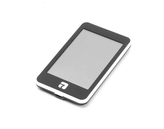
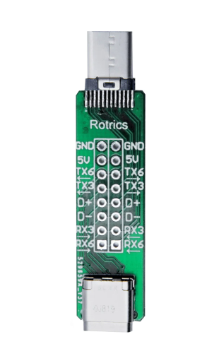
- 3.5' Rotrics
ESP32 3.5' (480x320) TFT
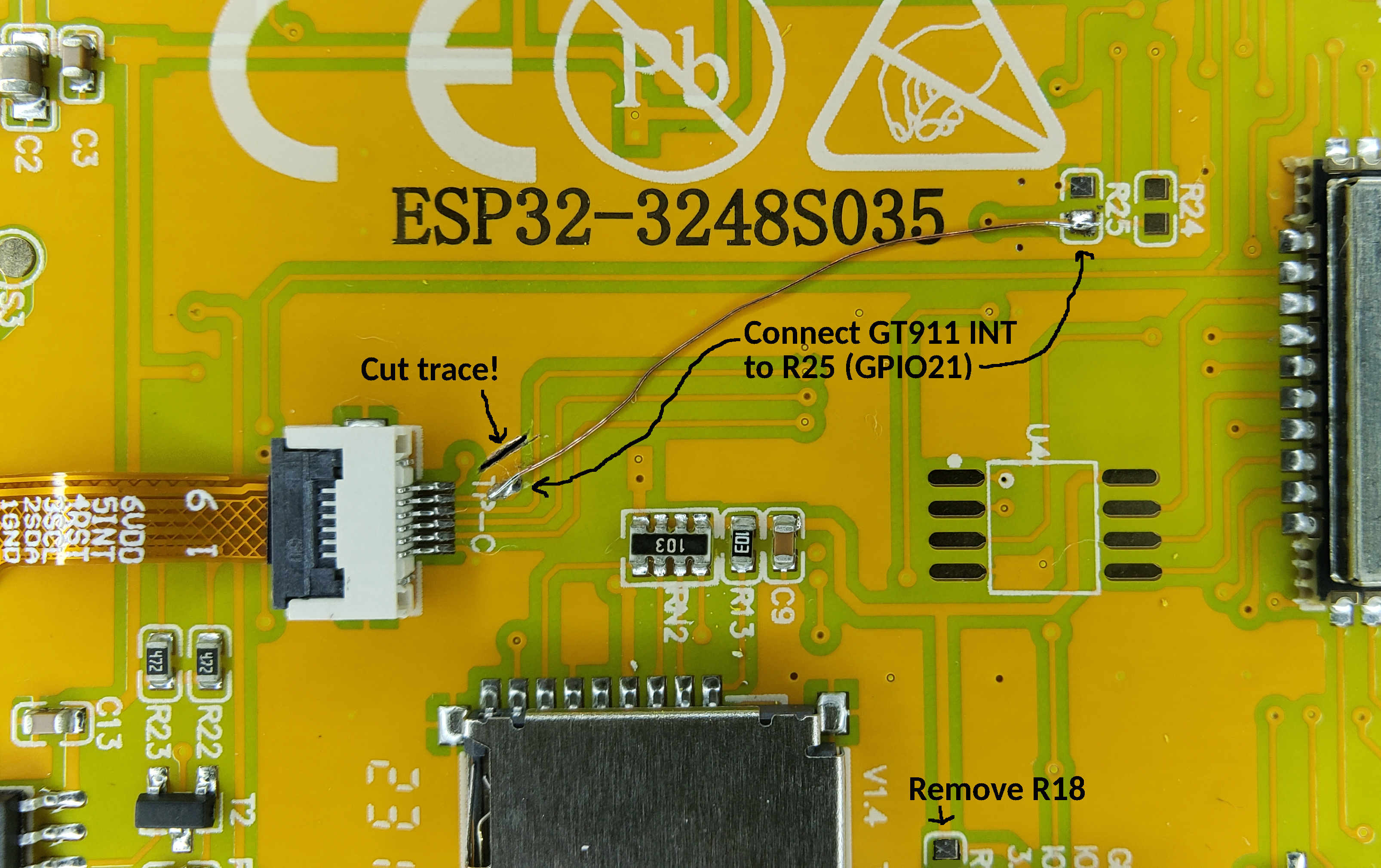
- 3.5' ESP32-3248S035R/C
ESP32 - 3.5' (480x320) TFT
- 2.8' ESP32-2432S028R
ESP32 - 2.8' (320x240) TFT
- 3.5' Rotrics
- ESP32-S3 boards
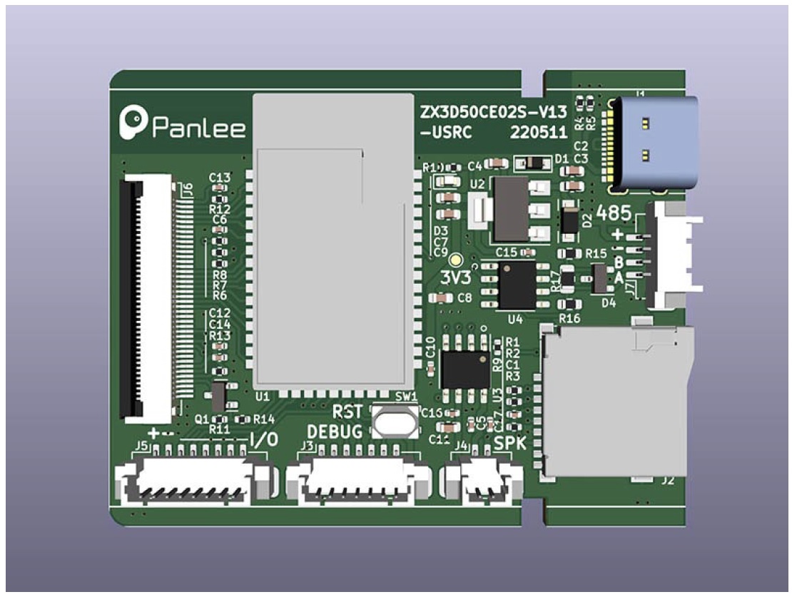
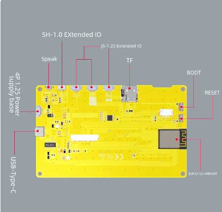
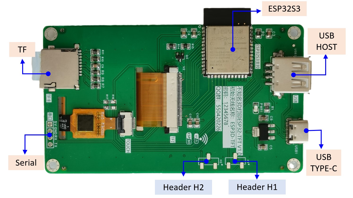
- 3.5' ZX3D50CE02S-USRC-4832
ESP32-S3 3.5' (480x320) TFT
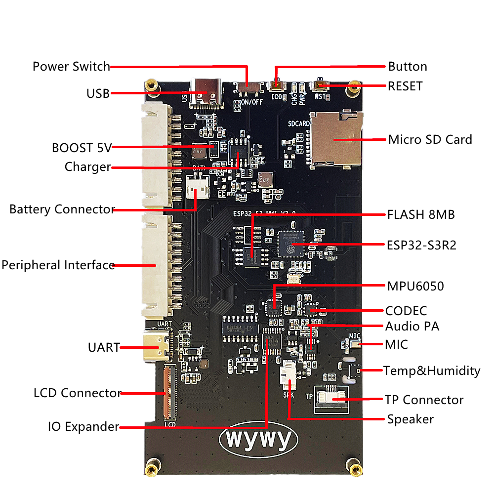
- 4.3' HMI-V3
ESP32-S3 4.3' (800x480) TFT
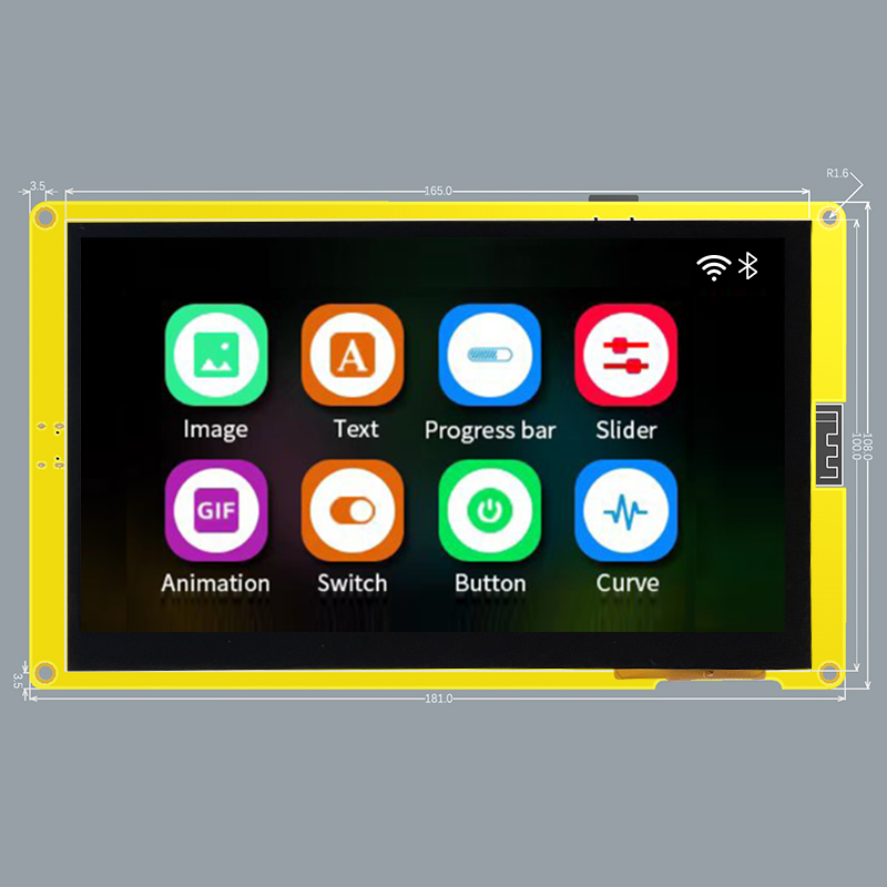
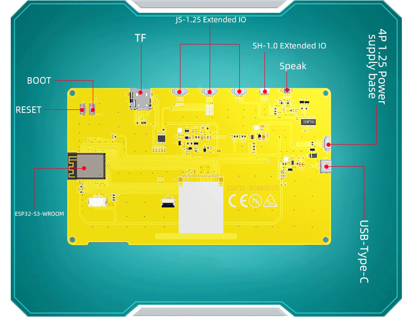
- 7.0' ESP32-8048S070C
ESP32-S3 7' (800×480) TFT
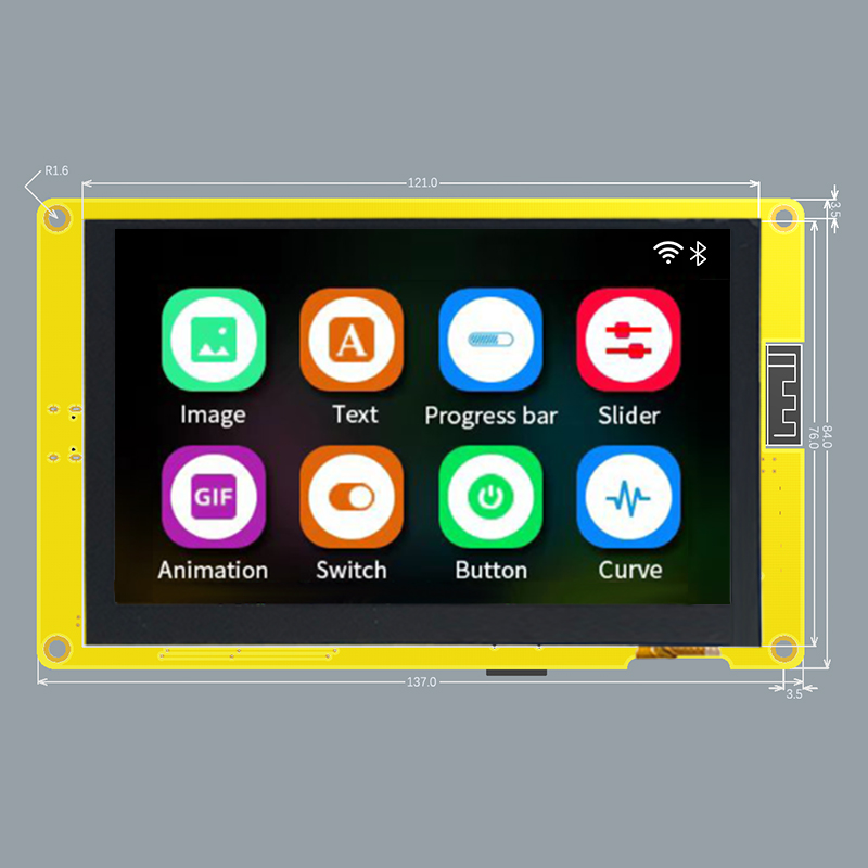
- 5.0' ESP32-8048S050C
ESP32-S3 5' (800x480) IPS TFT
- 4.3' ESP32-8048S043C
ESP32-S3 4.3' (800x480) IPS TFT
- 4.3' ESP32-4827S043R/C
ESP32-S3 4.3' (480x272) TFT
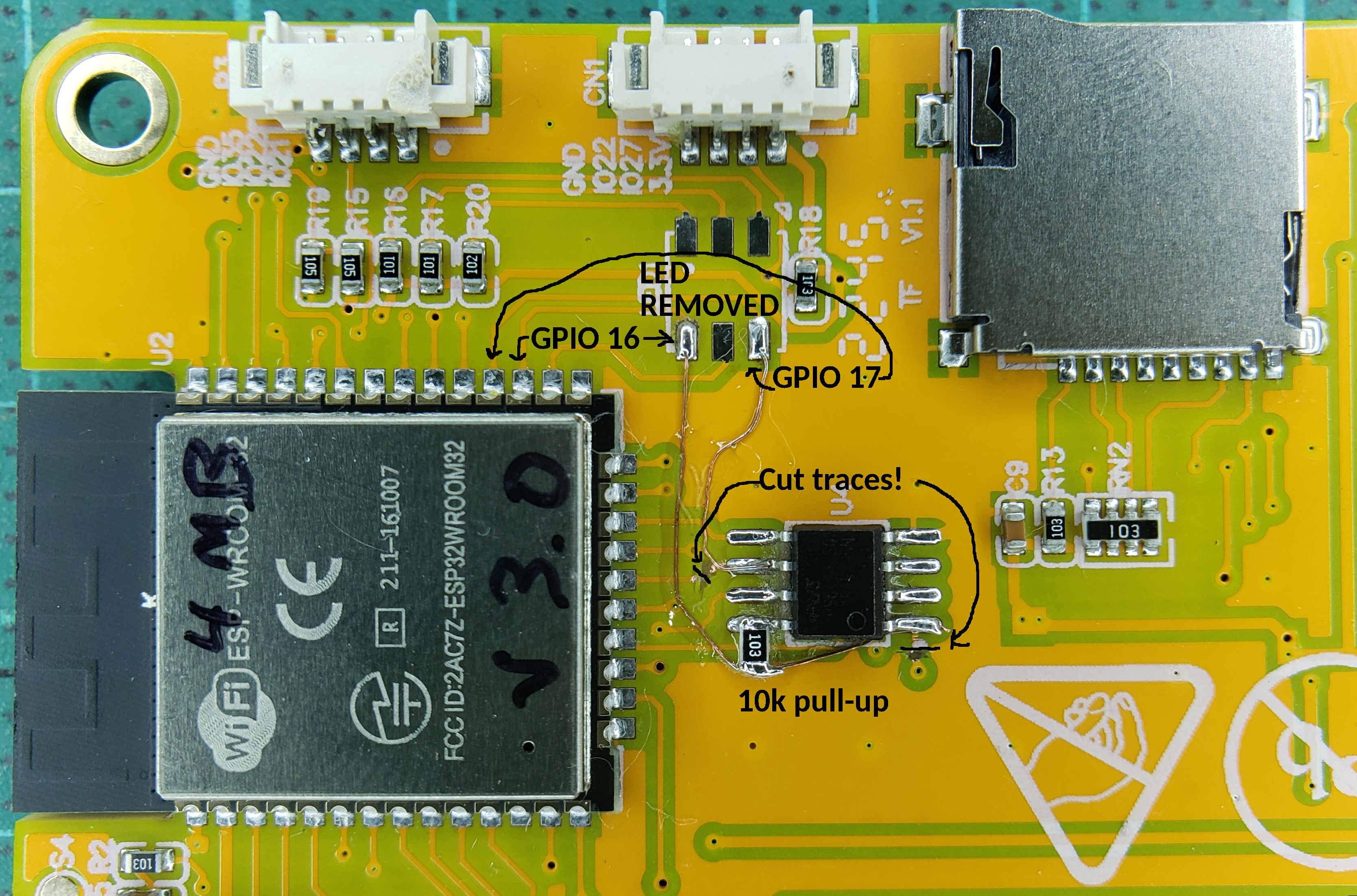
- 3.5' BZM-V1
ESP32 - 3.5' (480x320) TFT
- 3.5' ZX3D50CE02S-USRC-4832